
The universe is never truly still. Even in a vacuum, there are constant movements called quantum fluctuations. These are tiny, random changes in energy that exist everywhere. For a long time, scientists believed these fluctuations could be used to change the physical properties of materials. Recently, researchers from several institutions proved that the energy from a vacuum can indeed alter a nearby crystal. This was achieved by placing a very thin layer of one material on top of another without using any outside energy like light or heat. This research is published in Nature.
The researchers used a substance called hexagonal boron nitride, or hBN. This is a 2D material, meaning it is only a few atoms thick. They placed it on a crystal that is normally a superconductor. In this experiment, the hBN acted as a cavity, that is, a structure that traps and holds electromagnetic waves. Even when a cavity is empty, it still contains quantum fluctuations. When the hBN was added, the superconductivity in the crystal stopped. This happened because the tiny vibrations in the vacuum of the hBN matched the vibrations of the crystal, causing them to interfere with each other.
Controlling matter with the vacuum
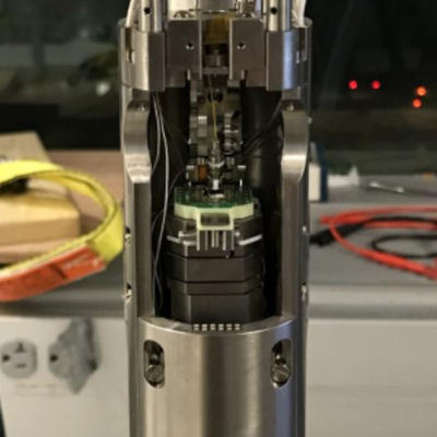
To prove this was happening without any outside interference, the group used a special magnetic microscope to look at the material in the dark. They found that the effect was much larger than they expected. The hBN is a hyperbolic material, which means it has a unique internal structure that makes vibrations grow much stronger. Because of this, the tiny energy changes in the vacuum were able to disrupt the movement of electrons in the crystal over a relatively large distance.
This discovery provides a new tool for engineering materials. In the past, scientists had to use lasers or high temperatures to change how a material works, but those changes often do not last. By using the natural fluctuations of the vacuum, these modifications can be more stable. In the future, this method could be used to control magnets or other electronic devices just by adjusting the thickness of a nearby 2D layer.