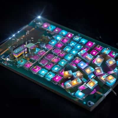

Researchers at ETH Zurich have shattered a significant technological barrier by developing organic light-emitting diodes (OLEDs) that are 50 times smaller than the current state of the art. Published in the journal Nature, this breakthrough was achieved using a novel, scalable manufacturing process that positions pixels just 100 nanometers apart, allowing them to interact and manipulate light in entirely new ways. [1]
The key innovation is a fabrication method using an ultrathin, resilient silicon nitride membrane as a nanostencil. This replaces the thick metal masks used in conventional OLED production, enabling the creation of pixel templates 3,000 times thinner. Researchers successfully demonstrated this by creating the ETH Zurich logo from 2,800 individual nano-OLEDs in an area the size of a single human cell. [2]
Crucially, at this scale, pixels can be placed closer together than the wavelength of visible light. This allows the light waves from neighboring pixels to interact, similar to ripples on a pond, enabling precise control over the light's direction and polarization. This capability unlocks applications far beyond ultra-sharp near-eye displays for augmented reality. [3]
The technology paves the way for advanced microscopic imaging, powerful miniature lasers, and novel sensors. It also introduces the possibility of "phased array optics," where light can be electronically steered without moving parts, a principle used in radar that could revolutionize optical computing and data transmission. The research, funded by a Swiss National Science Foundation Consolidator Grant, signifies a major leap toward integrating complex optical circuits directly onto computer chips.