
The electronics industry is hitting a wall with how many transistors they can fit on a single computer chip. Instead of making transistors smaller, they're now stacking them in layers like floors in a skyscraper. This means chips can process more data and do more complex tasks. But there's a problem: each layer includes a silicon wafer base. The silicon layer is thick and bulky, and slows down communication between layers.
MIT engineers have found a new way to stack chips without using these thick silicon bases. They describe their new method in a paper published in Nature. This new method lets them grow high-quality semiconductor layers directly on top of each other, even at low temperatures that don't damage the existing circuitry below.
Their technique involves growing materials on any type of surface, not just silicon. This direct layering makes communication between chip layers faster and more efficient. The researchers think this could make artificial intelligence (AI) hardware for laptops or wearables as powerful as supercomputers, with huge storage capabilities like data centers.
Enormous potential for the semiconductor industry
“This breakthrough opens up enormous potential for the semiconductor industry, allowing chips to be stacked without traditional limitations,” says study co-author Jeehwan Kim in an MIT press release. “This could lead to orders-of-magnitude improvements in computing power for applications in AI, logic, and memory.”
The new method uses very thin layers of materials called transition-metal dichalcogenides (TMDs), which are like super-thin sheets of atoms that can work well even when very small, unlike silicon.
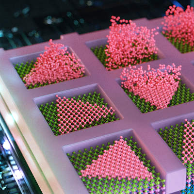
The engineers have managed to grow these TMDs at low temperatures by using a technique where atoms start to form crystals at the edges of small pockets on a mask, similar to how metal cools and forms in molds. This has allowed them to stack different types of TMDs, potentially doubling the number of transistors in the same space.
The team has already started a company, FS2, to turn this research into products. They aim to scale up and show how this can work in real AI chips.